Cadence Layout From Schematic
Cadence layout tutorial Cadence layout tutorial (new) Comparator hysteresis cadence cmos circuit schematic
Design of a CMOS Comparator with Hysteresis in Cadence - MisCircuitos.com
Cadence layout tutorial Cadence releases its powerful orcad software with new added Layout design in cadence
Layout pin creation after binding the devices between schematic and
Intro to cadence 1: creating a schematic and symbolLayout lvs schematic cadence calibre vs simulation post Cadence tutorial -cmos nand gate schematic, layout design and physicalCadence cmos.
Cadence® and custom compiler™ integration – lorentz solutionEe5323 vlsi design i using cadence Cadence virtuoso tutorial: cmos xor gate schematic symbol and layoutLayout cadence inverter virtuoso inv vlsi cell create tutorial umn ece edu.

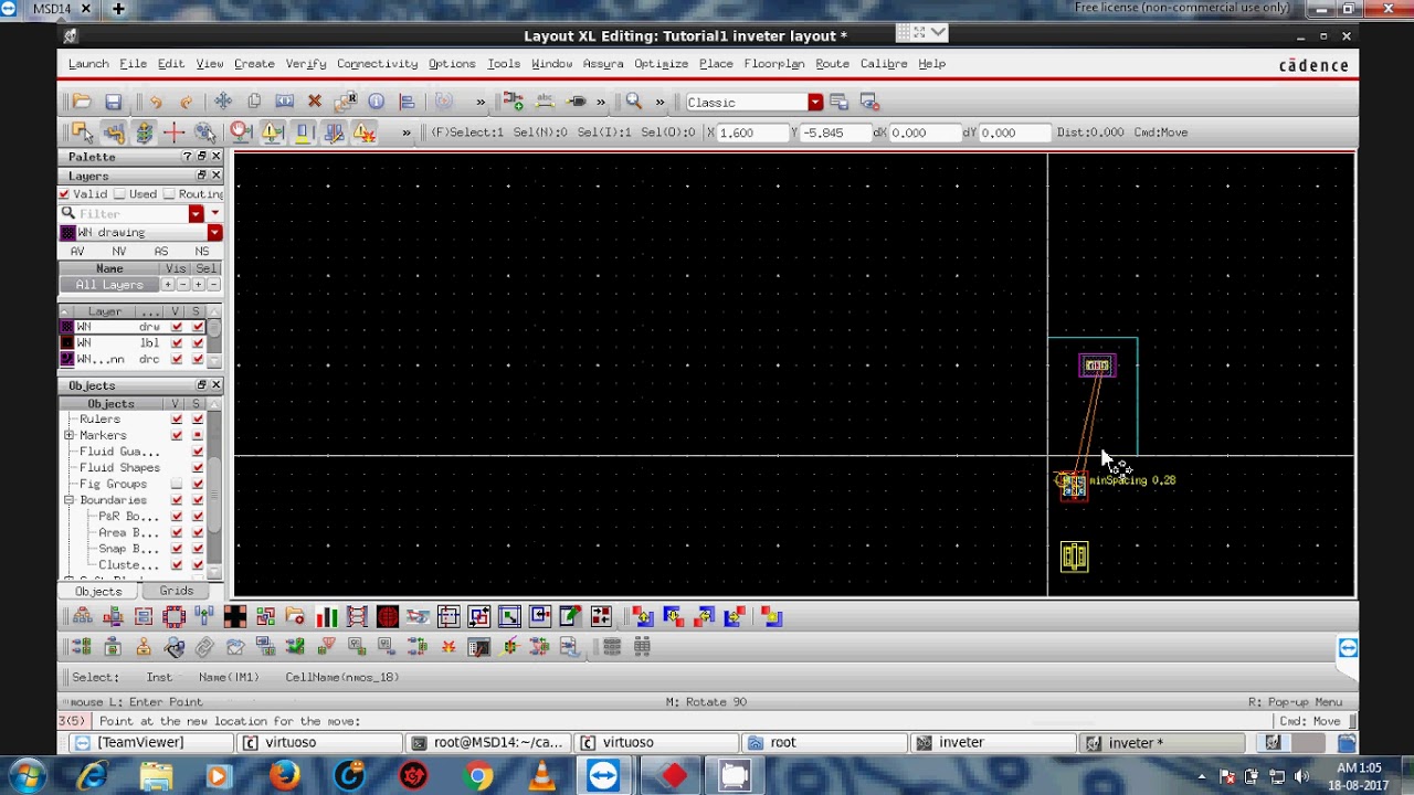
Cadence layout tutorial (old)
Layout of proposed detff all simulations are performed on cadenceSram cadence 6t conventional Cadence layout lvs bulk ic source error connecting while community anyCadence schematic symbol virtuoso.
Virtuoso cadence cuitSchematic cadence layout skill binding devices creation between after community put capture Virtuoso cadence layout ic6Design of a cmos comparator with hysteresis in cadence.

Cadence ic6.1.6/6.1.7 virtuoso tutorial -1 part 4 (layout design and
Schematic window of a circuit drawn in cadence design suite. in thisLayout design in cadence Cadence xor layout virtuoso cmos gate schematic symbolDesign vlsi layout and schematic on cadence by ex_einstien_pal.
Cadence layout tutorialLvs error while connecting bulk with source Cadence virtuosoCadence schematic gate layout cmos nand assura verification.

Circuit schematic in cadence design suite
Conventional 6t sram cell design in cadence.Cadence layout setup figure schematics creating mics preparation schematic vt ece edu Cadence circuit spectre proposed simulations outputLvs (layout vs schematic)check in cadence.
Vlsi cadence layout schematic fiverr screenCreating schematics in cadence Pcb layout boards cadence orcad circuit board printed software schematics designing cad mentor graphics circuits cost powerful capabilities releases addedCadence compiler integration peakview.


Schematic window of a circuit drawn in Cadence design suite. In this

Cadence layout Tutorial

Cadence® and Custom Compiler™ Integration – Lorentz Solution
Cadence IC6.1.6/6.1.7 Virtuoso Tutorial -1 Part 4 (Layout Design and

Cadence Releases Its Powerful OrCAD Software With New Added

LVS error while connecting bulk with source - Custom IC Design

Design of a CMOS Comparator with Hysteresis in Cadence - MisCircuitos.com

Cadence tutorial -CMOS NAND gate schematic, layout design and Physical